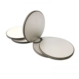
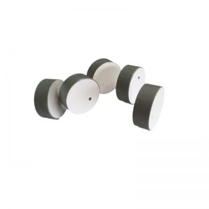
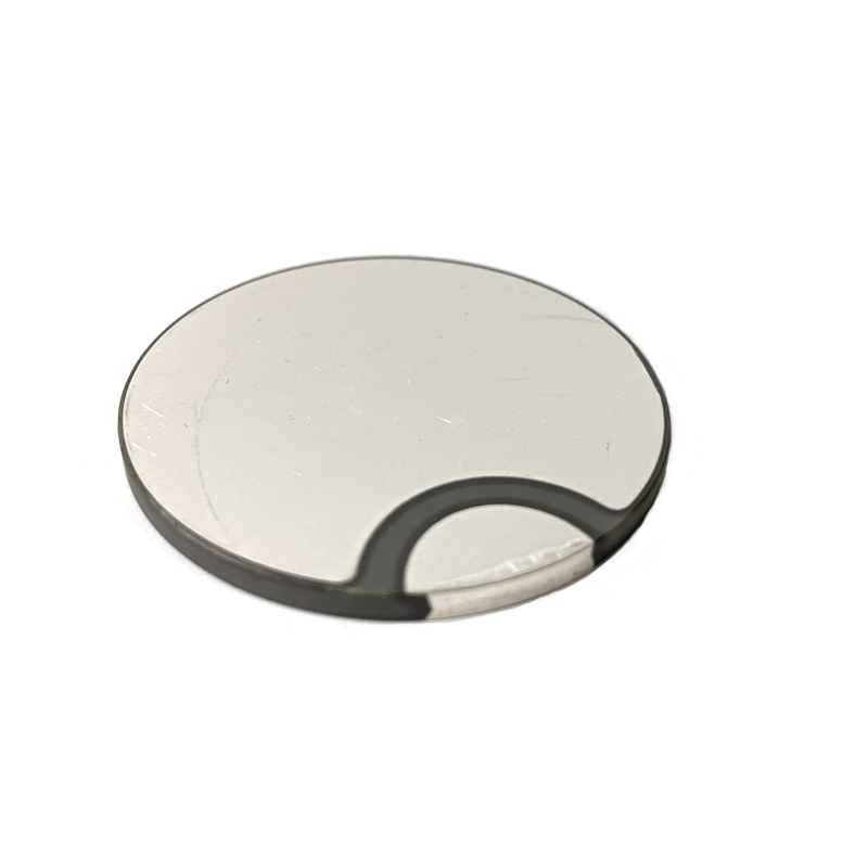
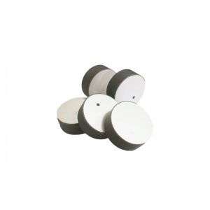
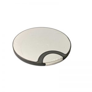
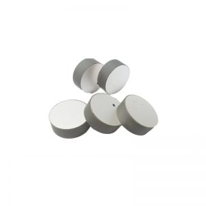
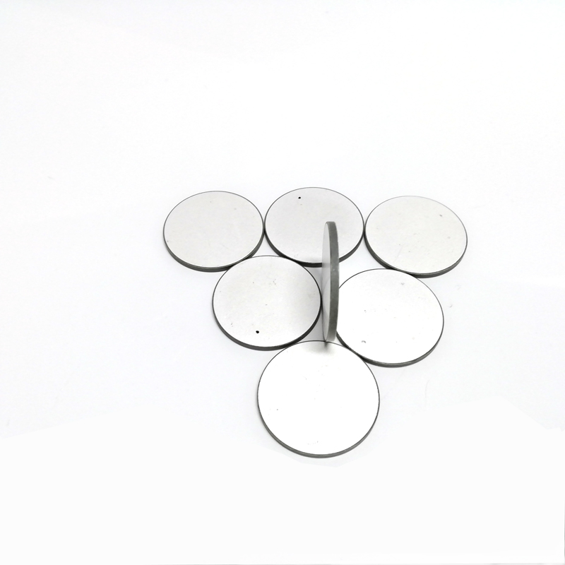
 Piezoelectric ceramic chips are materials that can convert mechanical energy into electrical energy, based on the piezoelectric effect. When piezoelectric ceramic chips are subjected to external forces, charges are generated on their surface, resulting in voltage generation. On the contrary, when a voltage is applied to the surface of a piezoelectric ceramic chip, mechanical deformation occurs inside. This characteristic makes piezoelectric ceramic chips widely used in fields such as vibration sensors, ultrasonic generators, and electronic instruments.
The manufacturing process of piezoelectric ceramic chips mainly includes steps such as batching, forming, sintering, and polarization.
1. Ingredients: Select appropriate chemical raw materials as needed, such as barium titanate, lead zirconate, и так далее., and mix them in a certain proportion.
2. Forming: Put the mixed raw materials into the mold and make a certain shape of the embryo through pressing or extrusion.
3. Sintering: Sintering the embryo at high temperature to make it a dense ceramic material.
4. Polarization: Polarize the sintered ceramic to give it a piezoelectric effect.
| Спецификация | Измерение (миллиметр) |
Радиальная частота (КГц) |
Емкость (±12.5%) pF |
Диэлектрический фактор диэлектрических потерьtanδ (%) |
Импеданс (Ω) |
Коэффициент электромеханической связиKr | Механический добротность (Качество) |
| ПЛС-QXJP3030 | Φ30×3.0 | 66.7 | 2730 | ≤0.3 | ≤15 | ≥0.55 | 500 |
| ПЛС-QXJP3530 | Φ35×3.0 | 63 | 3100 | ≤0.3 | ≤15 | ≥0.55 | 500 |
| ПЛС-QXJP3865 | Φ38×6.5 | 59.9 | 1580 | ≤0.3 | ≤15 | ≥0.55 | 500 |
| ПЛС-QXJP4530 | Φ45×3.0 | 50 | 5100 | ≤0.3 | ≤15 | ≥0.55 | 500 |
| ПЛС-QXJP4535 | Φ45×3.5 | 50 | 4700 | ≤0.3 | ≤15 | ≥0.55 | 500 |
| ПЛС-QXJP5030 | Φ50×3.0 | 46 | 5800 | ≤0.3 | ≤15 | ≥0.55 | 500 |
| ПЛС-QXJP5035 | Φ50×3.5 | 46 | 6300 | ≤0.3 | ≤15 | ≥0.55 | 500 |
| ПЛС-QXJP5050 | Φ50×5.0 | 46 | 4150 | ≤0.3 | ≤15 | ≥0.55 | 500 |
 Ультразвуковой преобразователь,Ультразвуковой генератор,Ультразвуковой очиститель -SKSONIC
